Other considerations such as which environment is each processor likely to be found, why particular performance enhancing methods have been used and where economies have been made, will be tackled and presented.
Although this is a technical report there will be a glossary of acronyms provided within the appendices.
1.0 – Brief History
1.1 – UltraSparc III cu
SPARC stands for Scalable Processor ARChitecture, which was first announced in 1987.
SPARC signifies an open standard, which is freely available through license from SPARC International, Inc. It allows companies to obtain a license, which gives them the right to manufacture and sell SPARC compliant processors[1].
By the early 1990s, SPARC processors were available from various vendors. In 1994, SPARC International, Inc. published The SPARC Architecture Manual, Version 9, which defined a powerful 64-bit enhancement to the SPARC architecture. The UltraSPARC III Cu is the latest product from the line of UltraSparc, which were the first family of SPARC-V9 compliant processors available from Sun Microsystems, Inc.
1.2 – Pentium 4
In 1971, The Intel Corporation introduced the world’s first microprocessor, which was to be the first in a long line of its microprocessor families. 1995 brought the introduction of the Pentium microprocessor, which was the first microprocessor of the Pentium family[2]. 1997 through to 1998, Intel broke the 200 MHz barrier and had already released its Pentium II and III processors respectively. With the continuing popularity of the home PC, Intel has continued to increase the performance and sales of the Pentium family. In 2000 the Pentium4 was launched.
2.0 – Overview & Features
2.1 – UltraSparc III Cu
The initial version of the UltraSPARC III processor was fabricated in a 0.18 m (Micron) process technology with aluminum (Al) metal layers. This technique allowed the processor to operate at frequencies of 600 MHz and 750 MHz. In the UltraSPARC III Cu, the aluminum technique has been replaced with 0.15 m Copper (Cu) metal layers to improve conductivity, the processor can now operate at frequencies of 900 and 1050 MHz. The UltraSparc III Cu is a 64-bit RISC processor, the RISC complies with Version 9 (V9) of the SPARC Instruction Set Architecture (ISA) and as such is upwardly compatible with earlier 32-bit versions of the SPARC ISA. As with previous versions of the UltraSparc, the latest version includes a special set of instructions to accelerate media and graphical applications, Sun Microsystems have named this feature Visual Instruction Set (VIS).
The processor can sustain the execution of up to four instructions per cycle, which is referred to as 4-way super-scalar processing. The chip supports a 64-bit virtual address space and a 43-bit physical address space. It has Level-1 instruction and data caches and support for a large external cache. The architecture is capable of operating in systems ranging from single processor workstations to production servers with multiple processors.
- 4-way super-scalar processor with nine execution units and six execution pipes.
- 14 stage, non-stalling pipeline.
- 64-bit data paths, 2 64-bit ALUs, 64-bit address arithmetic.
- 64-bit virtual address and 43-bit physical address space.
- Data pre-fetching mechanism.
- External Cache unit that supports a 2-way set associative cache.
2.2 – Pentium 4
The Pentium4 is based upon Intel’s 0.13 m and 0.18 m fabricated manufacturing process, offering clock speeds from 1.80 GHz to 2.80 GHz and 1.70 GHz to 1.90 GHz respectively. And is fully compatible with existing Intel® Architecture-based software.
The Pentium 4 is a 32-bit RISC processor and has a number of new features that Intel claim will advance performance over previous architectures. These new features marketed as the NetBurstä micro-architecture include an Execution Trace Cache, which is way to implement the level 1 instruction cache. It caches the decoded instructions thus removing the latency associated with the instruction decoder from the main execution loops. The processor has an enhanced floating-point and multimedia unit and a ‘hyper pipelined technology’. The hyper-pipelined technology basically doubles the pipeline depth found in the Pentium 3 from 10 stages to 20.
Other features include two Arithmetic Logic Units (ALUs), which are clocked at twice the core processor frequency and 128-bit floating-point registers. It also includes an enhanced branch prediction algorithm that has the net effect of reducing the number of branch miss-predictions by about 33% over the P6 generation processor’s branch prediction capability.
- 20 stage ‘hyper pipelined’ technology.
- 128-bit floating-point registers.
- Execution Trace Cache.
- 400 MHz system bus.
3.0 – Instruction Set Architecture
3.1 – UltraSparc III Cu
A fundamental feature of the UltraSparc III core is Instruction Level Parallelism (ILP). ILP allows multiple non-dependent operations to be executed simultaneously. Since the UltraSparc III contains independent execution units for operations such as MOV (transfer instruction) and SUB (Integer Execution Instruction), several instructions can be executed concurrently. With this parallel execution technique, a programmer can achieve true ILP. Another feature of the V9 ISA is that there are data pre-fetch instructions. These instructions allow software to give warning to hardware that it will be using data in the future.
An addition to the V9 architecture are the Visual Instruction Set (VIS) which uses a series of specialized commands to complete normally CPU intensive graphic operations. VIS addresses performance concerns by dividing standard floating-point graphic operations across the entire scope of the integer and floating-point execution units. VIS operations rely on integer registers for loading and storing data, while floating-point registers provide power for data manipulation.
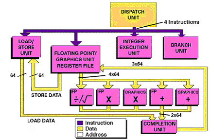
Figure 1. The floating-point unit supports five different functions including two specifically tailored for graphics (courtesy of http://sunsite.ics.forth.gr)
An UltraSPARC III Cu processor contains 160 general-purpose 64-bit r registers. The registers in the floating-point register set (also used for VIS and block load store instructions) are combined in specific ways to support data sizes up to 128 bits. All integer registers and the upper floating-point registers are 64 bits wide.
3.2 – Pentium 4
IA32 is the name used by Intel to describe their 32-bit instruction set architecture. The Intel NetBurst micro-architecture supports the entire IA32 instruction set including Intel’s MMX™ technology and the Streaming SIMD (Single Instruction Multiple Data) Extension.
An additional 144 instructions called the Streaming SIMD Extensions 2 or SSE2 have been added that compliment MMX technology and SSE instructions by supplying increased computation capability, support for larger data types (e.g. double precision floating point numbers and 64-bit packed integer numbers), new cache and memory management instructions and several data handling and conversion instructions. In addition to these, the Pentium4 has enhanced its floating-point unit from its predecessors P6 architecture.
- 8 general-purpose registers, 32-bit
- 6 segment registers, 16-bit
- 8 floating-point and 8 MMX registers, 64- bit
- 8 XMM registers for SSE operations, 128-bit
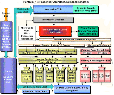
Figure 2. Pentium 4 Architectural diagram. (Courtesy of www.tomshardware.com)
3.3 – Comparison
The first obvious difference between the two processors is the mammoth divide in clock speeds, with the P4 (Pentium 4) offering up to 2.8GHz and the U3 (UltraSParc III) offering up to 1050 MHz. Although I will tackle this later on, the difference in speed is does not offer a linear-increase in performance. The second obvious difference is the 32-bit and 64-bit architecture from the P4 and U3 respectively. 32-bit operations can affect calculations, memory capacity, and storage access. Although the P4 has implemented 64-bit and 128-bit floating point registers, because of the 32-bit data bus it takes at least 2 clock cycles to fill a 64-bit line. Whereas the U3, being a 64-bit processor, can fetch and execute data in 64-bit blocks at least once per clock cycle (without taking into account any super-scalar processing).
The P4 has huge instruction set with well over 300 instructions, compared to just under 200 instructions within the U3. Many additional instructions have been added to the P4 instruction set that are focused on dealing with floating point calculations, that would be mostly used in multimedia applications. The U3 has a similar dedicated set of instructions for this purpose, which Sun have named the ‘Visual Instruction Set’ or VIS. Although the U3 may not have as many instructions to deal with floating point calculations, the U3 has 2 floating point units which can provide simultaneous execution on the floating point instructions, as opposed to the P4’s 1 floating point unit. Although both processors have twin ALU’s, it seems that the U3 generally has many more registers, for example there are 160 general purpose registers compared to the P4’s 8.
There are scalability issues because the P4 is a uni-processor design, meaning it can only support one processor, whilst the U3 can support multiple processors.
4.0 – Cache Design
4.1 – UltraSparc III Cu
The UltraSPARC III supports two levels of cache memory. The first level (L1) consists of four separate caches, two large and two small. The second level (L2) consists of a single large cache. The two large L1 caches store instructions and data, respectively. The two smaller L1 caches are: 1.) A pre-fetch cache which stores predicted load instructions. 2.) A write cache, that aims to reduce the amount of storage bandwidth required. All four L1 caches are on-chip. The L2 cache consists of a combined instruction and data cache. The contents of the L2 cache are stored off-chip in Static RAM, but the L2 address tags are kept on-chip for faster access.
· The Instruction cache is 32 KB in size, 32-byte line size (eight instructions) and implements the 4-way set associative mapping function.
- The Data cache is 64 KB in size and implements a 4-way set associative mapping function. The data cache uses a write-through policy to replace lines of 32-bytes in size.
- The Pre-fetch cache is 2 KB in size and implements a 4-way set associative mapping function which uses a write- through policy.
- The Write cache is 2 KB in size and implements a 4-way set associative mapping function. The line size is 64 bytes with 32-byte sub-blocks and uses a write-back policy.
- The L2 cache can connect to up to a maximum of 8 MB, implements an 2-way set associative mapping function and uses a write-back policy.
Figure 3. U3 Cache Design. (Courtesy of www.sun.com)
4.2 – Pentium 4
The Pentium 4 also supports 2 levels of cache memory. The first level (L1) consists of two small caches, a Data cache and an Instruction cache. The second level (L2) consists of a single medium size cache. The first small L1 cache is a Data cache and is 8-KB in size has a 4-way set associative mapping function with an 64-byte line size. Interestingly, the capacity has been reduced in size by 50% from the Pentium 3 processor. The second small L1 cache is what Intel refer to as the ‘Trace Cache’, which is basically a code cache for decoded micro-ops, is 12-KB in size has a 4-way set associative mapping function. Rather than constantly decode the instructions in a loop over and over again, it caches the output of the decoder, caching the raw micro-ops. Both L1 caches implement a write-through page replacement policy.
The L2 cache holds both data and instructions, is 256-KB in size, has an 8-way set associative mapping function with a 128-byte line size (two 64-byte blocks) and implements a write-back page replacement policy.
- The Data cache is 8 KB in size and implements a 4-way set associative mapping function. The data cache uses a write-through policy to replace lines of 64-bytes in size.
- The Instruction cache (Trace cache) is 12 KB in size and implements the 4-way set associative mapping function, also uses a write-through page replacement policy to replace 32-byte lines.
- The L2 cache (on chip) is 256 KB in size, has an 8-way set associative mapping function with a 128-byte line size. Implements a write-back page replacement policy.
Figure 4. P4 Cache Design. (Courtesy of www.hardware.fr)
4.3 – Comparison
4.3.1 – Overview
Both processors employ a multi level cache, utilising a level one and level 2 cache design. At a glance, the most striking difference between the two designs is in the storage capacity, with the UltraSparc having a whooping optimum capacity of 8 MB, opposed to the Pentium 4’s 256 KB. Both designs also have a Data and Instruction cache, but the UltraSparc has the added units of a Write and Pre-fetch cache. At further inspection, it becomes clear how much the two Cache Designs differ.
4.3.2 – Level 1 Cache
Both processors have a Data cache, the UltraSparcs capacity is larger at 64 KB compared to the Pentium 4’s smaller 8 KB. Also, the Pentium 4 Data cache has 4-way set associative mapping with 64 Byte lines (8 * 64 line block) as opposed to the UltraSparcs 4-way set associative mapping with 32 Byte lines (8 * 32 line block).
The Pentium ‘trace cache’ is basically a code cache for decoded micro-ops. Rather than constantly decode the instructions in a loop over and over again, the Pentium 4 caches the output of the decoder in a 12 KB cache. It offers a line size of 32 Bytes and 4-way set associative mapping (4 * 32 Byte Block). The UltraSparc III has an almost identical Instruction cache except for its larger 32 KB capacity. As explained below, the higher Line size does not necessarily result in superior efficiency, on the contrary, hit ratios may be decreased.
Both L1 Cache designs employ the same write-through policy, which can cause more memory writes and thus prove slower than write-back policy (which only writes when a cache line is rejected) used on both the processors L2 cache design.
4.3.3 – Level 2 Cache
Quite an obvious advantage of the Pentium’s Cache design is the on-chip L2 cache, which takes advantage of the principle of locality, as opposed to the UltraSparc’s external L2 cache. A fine balance of line size is needed to maximize the hit rate, with this said, the Pentium 4’s L2 cache has 8-way set associative mapping with 128 Byte lines (8 * 128 Byte lines per set or block). Not only is the overall capacity vastly smaller than the UltraSparc, but the block size of 8 lines multiplied by 128 Bytes is quite large and once again, using the principle of locality, may tip the balance of the probability of referencing all the data held in that block, which may ultimately decrease the Pentiums hit ratio.
5.0 – Pipeline Architecture
5.1 – UltraSparc III Cu
To improve performance and in particular clock speed, the Sun Designers have implemented a deep execution pipeline within the UltraSparc III Cu. As a consequence, the design is able to scale up from its initial frequency of 600 MHz to its current frequency of 1050 MHz.
The processor’s fetch execute cycle has been segmented into 14 separate stages, as can be seen in figure 5, elementary processes such as instruction fetch and store have been fragmented into smaller individual processes, as a consequence, will reduce dead time.
The UltraSparc employs several separate pipelines, each dedicated to the execution of a particular class of instruction. For example, the execution process (stage 8) of the pipeline can simultaneously execute 4 instructions, possibly to one of the 4 Integer units or one of the two ALU’s (dependant on availability). This design is known as ‘Super-scalar’, because of the processors ability to issue 4 instructions simultaneously and process them in parallel, it is known as 4-way Super-scalar.
To reduce the risk of stalling, the processor implements an advanced branch prediction mechanism based on 4 KB’s of stored branch history that accurately predicts whether or not a branch will be taken about 95% of the time[3]. Wrong predictions have a penalty of 7 cycles, required to back up, fetch the branch instruction again, and start over.
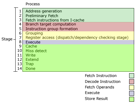
Figure 5. UltraSparc III Cu 14-stage pipeline architecture
5.2 – Pentium 4
To increase clock speed, Intel has implemented an extremely deep instruction pipeline, resulting in clock rates of 2GHz and above. The fetch execute cycle has been segmented into 20 separate stages and as can be seen in figure 6, all elementary processes are fragmented except for the store process which is excluded from ‘Hyper Pipeline’.
The Pentium 4 pipeline can keep up to 126 instructions ‘in-flight’, amongst them up to 48 load and 24 store operations. The L1 ‘Trace Cache’ helps reduce the risk of stalling (as detailed in section 4.2).
An improved branch prediction algorithm has been implemented minimise pipeline flushes. There is also a 4KB branch predictor table, which is eight times larger than that included in the Pentium 3. Intel estimates that the new branch prediction will reduce wrong predictions by one-third.
Stage Pipeline Process:
1 – 2 Branch prediction supplies address of the next micro-op (TC Nxt IP).
3 – 4 Micro-ops are fetched (TC Fetch)…
5 and transferred (Drive)…
6 into the RAT (register alias table). Allocation of data (Alloc)
7 – 8 logic registers rename (Rename).
9 Micro-ops are put in the Queue until there appears…
10 – 11 – 12 free place in the Schedulers.
13 – 14 There, dependencies are to be solved and then micro-ops are transferred to the register files of the corresponding Dispatch Units.
15 – 16 Micro-op is executed, and Flags are calculated.
17 – 18 When implementing the jump instruction…
19 the real branch address and the predicted one are to be compared (Branch Check).
20 After that the new address is recorded in the BTB (Drive).
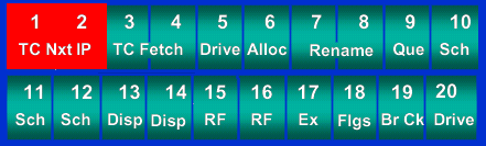
Figure 6. Pentium 4 20-stage pipeline Architecture (Courtesy of www.digit-life.com)
5.3 – Comparison
The main benefit of a longer pipeline is the ability to process more instructions in fewer clock cycles and it seems Intel have implemented this theory to achieve its higher megahertz ratings. The problem with this design is that the Pentium 4 requires more cycles to complete a given instruction than the shorter UltraSparc pipeline design. Further more, if miss-predictions occur, the whole pipeline needs to be flushed and refilled. The longer the pipeline the more ‘in-flight’ instructions will be lost and the longer it takes until the pipeline is filled again.
More over, the P4 has a minimum miss-predict penalty of 19 clock cycles for code that’s in the L1 cache as opposed to the UltraSparcs’ 7 clock cycle penalty. However, both processors implement a 4KB branch history mechanism that ensures an extremely high percentage of correct branch prediction.
Another consideration worth mentioning is the fact that the UltraSparc III Cu is a 4-way Super-scalar design, allowing 4 instructions (and at certain stages up to 8) to be processed simultaneously. By comparison, the P4 can process a maximum of 3 instructions per cycle (IPC), limited by its maximum of 3 parallel units.
One minor flaw in the UltraSparc pipeline architecture was discovered shortly after the release of the chip, Sun Microsystems announced that a design fault in the current UltraSparc III chip had been found that meant a pre-fetch pipeline must be disabled for the chip to correctly handle floating-point calculations[4].
6.0 – Conclusion
The Intel Pentium family of processors have enjoyed widespread use in the majority of home PC’s, with the ever increasing demand and use of multimedia applications in the home and the fact that high clock speeds sell, the Pentium 4 processor has been designed with these goals in mind. The UltraSparc III Cu on the other hand, is commonly found in an enterprise network computing environment. The UltraSparc III is essentially designed to work in systems ranging from single processor workstations through to cache coherent servers with over a hundred processors. Not only that, but Sun Microsystems specifically direct their hardware and thus the UltraSparc III processors towards the business market.
The Pentium 4 offers extremely high clock rates, which have been achieved by primarily redesigning and increasing the pipeline depth. The 20-stage pipeline does not come without its drawbacks, especially if the pipeline is not provided with a constant stream of instructions. Other additions include an increased instruction set (SSE2) aimed at multimedia specific computation such as 3D pixel rendering. The introduction of a ‘Trace Cache’ which has resulted in a decrease in the P4 L1 cache to only 8 KB (half the size of its predecessor), but as a trade off, Intel was probably forced to reduce the size of the L1 data cache to enable its extremely low latency of only 2 clock cycles.
The UltraSparc III Cu processor is a high-performance, super-scalar processor that implements the 64-bit SPARC-V9 RISC architecture. It can sustain the execution of up to four instructions per cycle, even under conditional branches and cache misses, mainly because the units are asynchronously supplied instructions and data to the rest of the pipeline. As with the P4, the U3 has an increased instruction set (VIS) aimed at multimedia specific computation, although not achieving as impressive clock rates as the P4, the U3 has the benefit of being 4-way super-scalar.
In essence, both processors have been designed to work within completely different environments, although from a marketing point of view, both processors have to be seen to deal with any computing situation. A particular task initiated on one processor may out perform the other and vice versa, essentially it’s a matter of using a specific processor for a certain type of application to gain the best results.
Appendix A – Performance Benchmarks
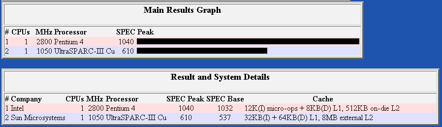
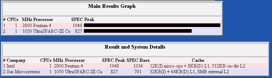
The following benchmarks are taken from the SPEC®cpu system and are probably the most frequently referenced benchmarks in the computing industry. It is a suite of tests that is developed by the Standard Performance Evaluation Corporation (SPEC, http://www.spec.org). The suite is based on real applications and is divided into two categories; Integer (MIPS) and Floating point (GFLOPS).
Integer (SPECint®2000)
Floating point (SPECfp®2000)
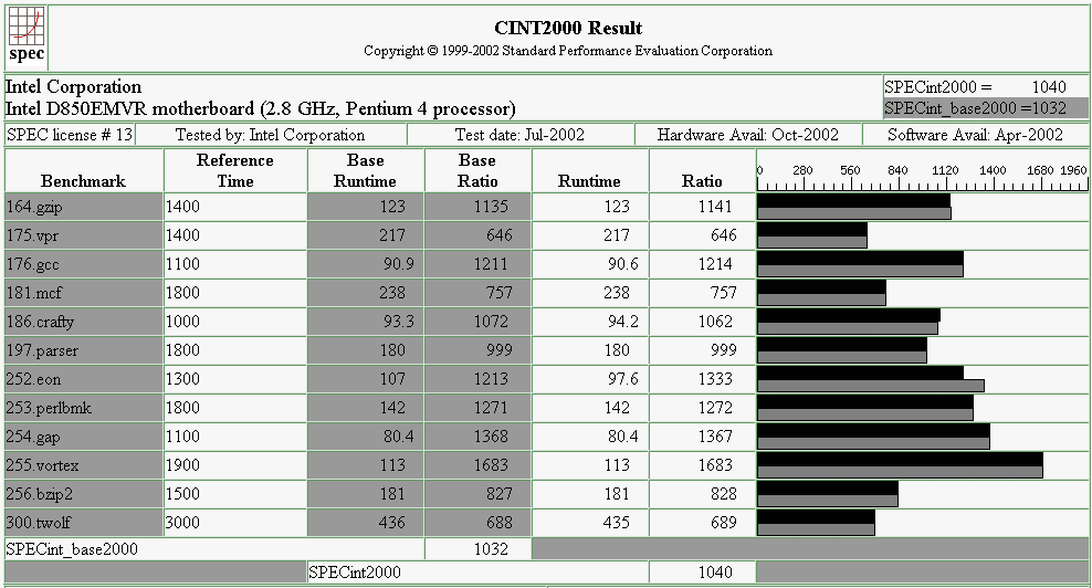
Pentium 4 Integer Results
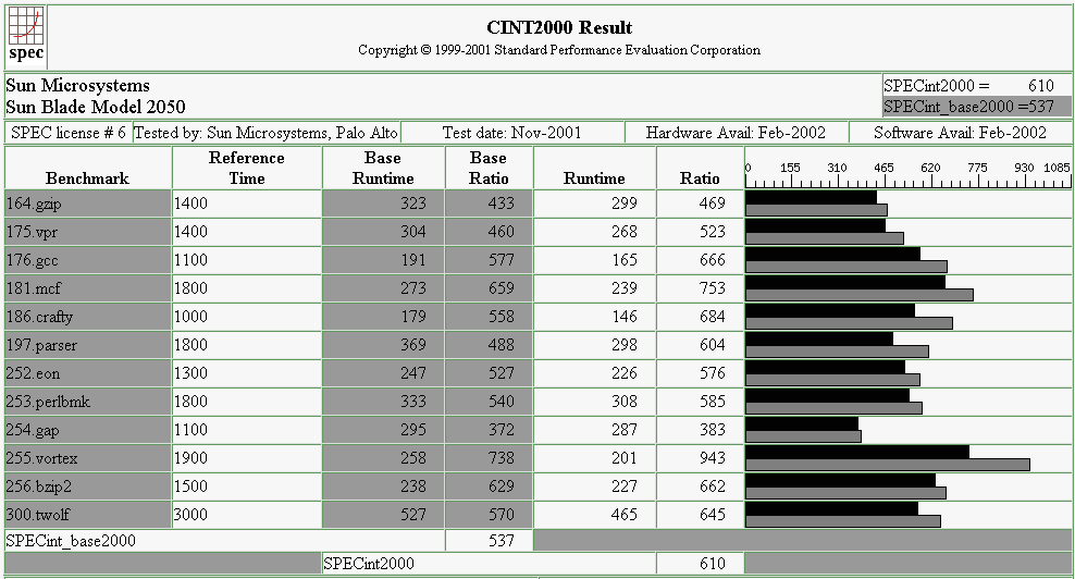
UltraSparc III Cu Integer Results
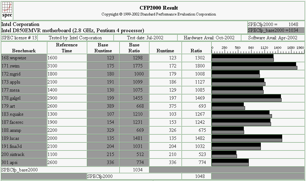
Pentium 4 Floating-Point Results
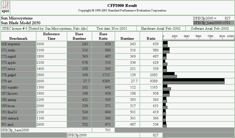
UltraSparc III Cu Floating-Point Results
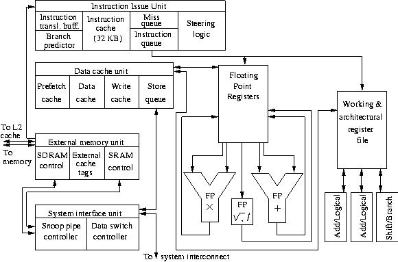
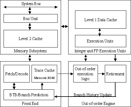
Appendix B – Block Diagrams
UltraSparc III Cu Basic Block Diagram
Pentium 4 Basic Block Diagram.
Appendix C – Glossary of Acronyms
ALU Arithmetic Logic Unit
CISC Complex Instruction Set Computer
CPU Central Processing Unit
CU Control Unit
DRAM Dynamic Random Access Memory
FP Floating Point
GFLOPS Giga FLoating point Operations Per Second
GHz Giga Hertz
IA – 32 Intels’ 32-bit Instruction set Architecture
ILP Instruction Level Parallelism
IPC Instructions Per Cycle
ISA Instruction Set Architecture
KB Kilobyte
L1 Level one cache
L2 Level two cache
MFLOPS Mega FLoating point Operations Per Second
MHz Mega Hertz
MIPS Millions of Instructions Per Second
MB Megabyte
RAM Random Access Memory
RISC Reduced Instruction Set Computer
SDRAM Synchronous Dynamic Random Access Memory
SIMD Single Instruction stream-Multiple Data stream
SSE2 Streaming SIMD Extension 2
SPARC Scalable Processor ARCitecture
SRAM Static Random Access Memory
VIS Visual Instruction Set
Bibliography
Books
Computer Architecture design and performance – B. Wilkinson, Prentice Hall 1996
Computer Organisation and Architecture – B.S. Chalk, Macmillan 1996.
High-Performance Computer Architecture – H.S. Stone, Addison-Wesley 1993
WWW
http://www.intel.com
http://www.intel.com/design/Pentium4/prodbref/
http://intel.com/technology/itj/q12001/articles/art_2.htm
http://www.sun.com
http://www.sun.com/processors/UltraSPARC-III/
http://www.sun.com/processors/whitepapers/index.html#III
http://www.sun.com/processors/UltraSPARC-III/USIIICuoverview.pdf
http://www.sparc.org
http://www.anandtech.com/showdoc.html?i=1360&p=15
http://www.emulators.com/pentium4.htm
http://web.archive.org/web/20030519220247/http://meseec.ce.rit.edu:80/eecc550-spring2002/550-3-20-2002.pdf
http://www.arstechnica.com/cpu/01q2/p4andg4e/p4andg4e-1.html
http://www.aceshardware.com/Spades/read.php?article_id=20000190
http://www.emulators.com/pentium4.htm
http://www.netsoc.tcd.ie/~nickm/4ba2/performance/mythicalmegahertz.pdf
http://www.chipcenter.com/eexpert/dgilbert/dgilbert074.html
http://www.dell.com/us/en/gen/topics/vectors_2001-pentium4performance.htm
http://sysopt.earthweb.com/articles/usparc-3/index6.html
http://web.archive.org/web/20080911155138/http://www.eng.dmu.ac.uk:80/~pdn/UltraSPARC/ultra_arch_architecture.html
http://web.archive.org/web/20031206201454/http://www.ee.princeton.edu:80/~xzhu/p4.html
http://www6.tomshardware.com/cpu/00q4/001120/p4-05.html
http://www.cs.berkeley.edu/~pattrsn/61CF00/lectures/lec23-x86.pdf
http://www.euro.dell.com/countries/eu/enu/gen/topics/vectors_2000-pentium4.htm
http://www.owlnet.rice.edu/~elec525/lectures/lecture02.pdf
https://web.archive.org/web/20081121160923/http://www.digit-life.com/articles/pentium4/index2.html